| homepage of Michael Dietmar Pierschel |
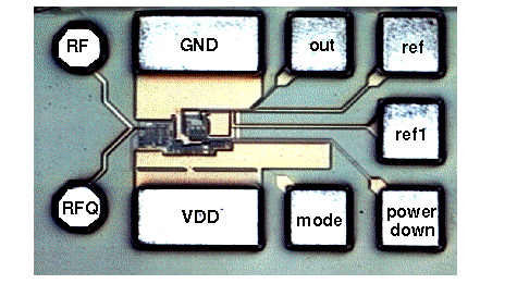
CMOS prescaler
Messbericht (Doku nicht online verfügbar)
designed circuit reference (Doku nicht online verfügbar)
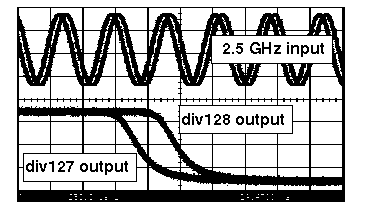
Dual Modulus Prescaler operate @ 2.5GHz / 15mW total power
There exist timing problems in the actual circuit implementation. Therefore the division ratio of 128/129 is reduced to 127/128. Measurements with cooled chips deliver a normal circuit operation. These problems have been verified in simulation and fixed in a first redesign in June 1999.
The best value in literature reference for CMOS is 24 mW@3V and 1.8 GHz [48].
Dual Modulus Prescaler Single Ended Input Sensitivity vs. Frequency
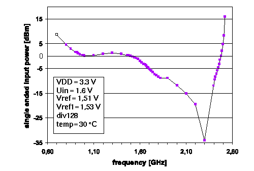
The sensitivity depends on actual operating point setting.
fmax=5.11GHz/div128@12dBm input
fmax=4.50GHz/div129@12dBm input
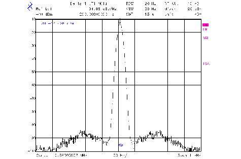
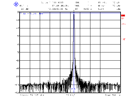
The phase noise is below -94 dBc/Hz @ 100 Hz distance.
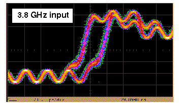
Dual Modulus Prescaler operate @ 3.8GHz / 10.75mW total power. The input signal feed through to the output signal. One of the internal low speed flip-flop do not work, since this design has been optimized for 350 nm technology. So the division ratio is 64/65 here instead of 128/129. The high speed block has no timing problems due to the faster transistors in this technology.
Dual Modulus Prescaler Single Ended Input Sensitivity vs. Frequency
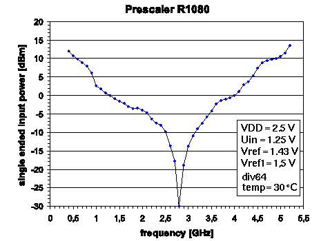
fmax=6.65GHz/div64
fmax=5.56GHz/div65
The phase noise is below -82 dBc/Hz @ 10 Hz distance.
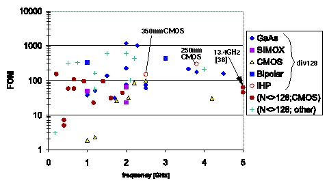
criterium minimum power
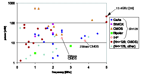
criterium best FOM
Kontakt: mailto: 