
CMOS prescaler basics
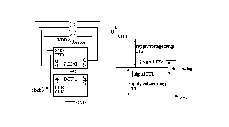
Conventional Type
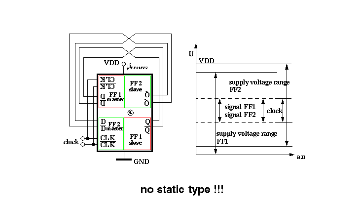
CMOS Stacked Flip-Flop Type
Full CMOS Crossed Flip-Flop Type
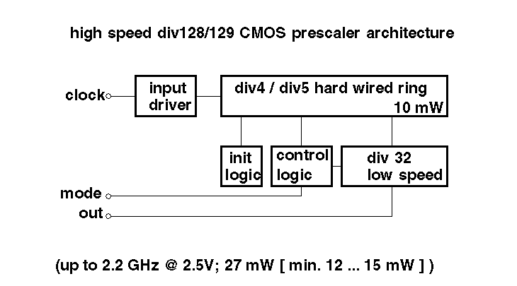
Common Dual Modulus Divider Architectures
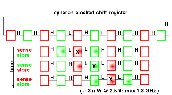
Shift Register Architectures
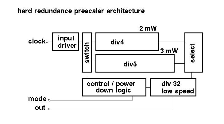
Hard Redundance Architecture
Cycle Stealing Architecture
Power Save Techniques
Next Steps
Technology Tests
the frequency range up to 2.5 GHz can be adressed with 250 nm CMOS
With reduced parasitics 60 fF instead of 100 fF per switching node
signals up to 3 GHz have been processed correct in the simulation.
the power requirements fall below 1 mW per FF
( without current save techniques )
the delay time of 250 nm p- and n-channel transistors are nearlythe same
check the model accuracy in the 1...3 GHz range
check if ballistic charge transport becomes dominant in the 250 nm
channel length region
enhanced drift fields in the p-channel transistors due tu a burriedchannel technology
back to top
Standard CML Flip-Flop's
Conventional Type

Stacked Flip-Flop's
HCrossed Flip-Flop's
back to top
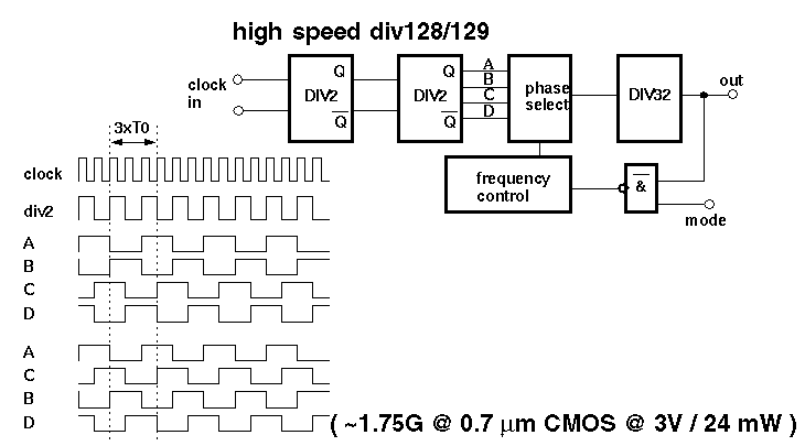
Common Dual Modulus Divider Architectures
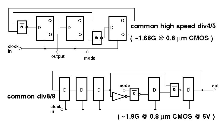
Common Dual Modulus Divider Architectures
back to top
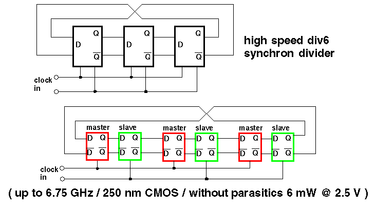
Synchron Johnson Counter's
back to top
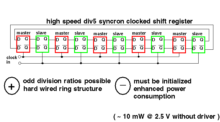
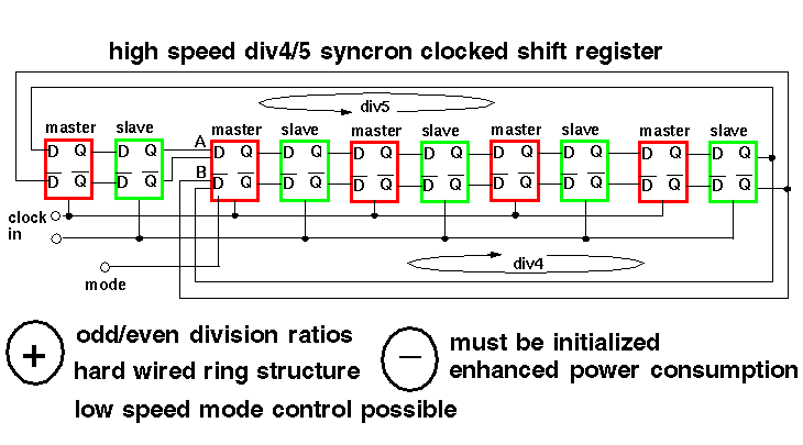
Shift Register Architectures
back to top
Power Save Technique
back to top
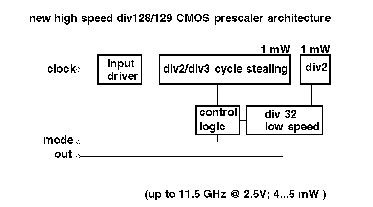
New Prescaler Architectures
back to top
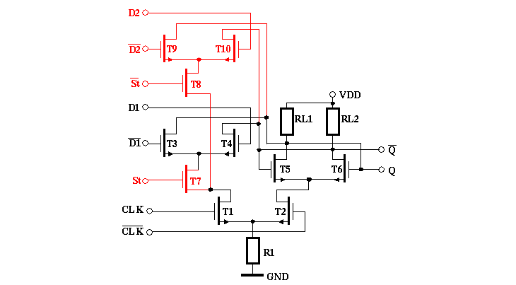
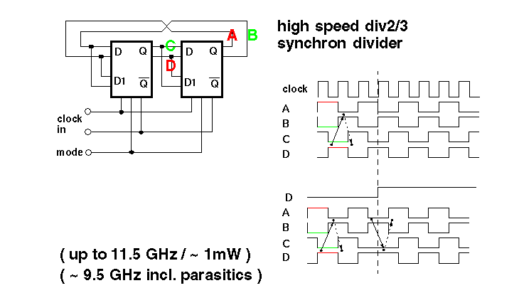
modified D-FF
cycle stealing method
back to top
Proposed Architecture
back to top
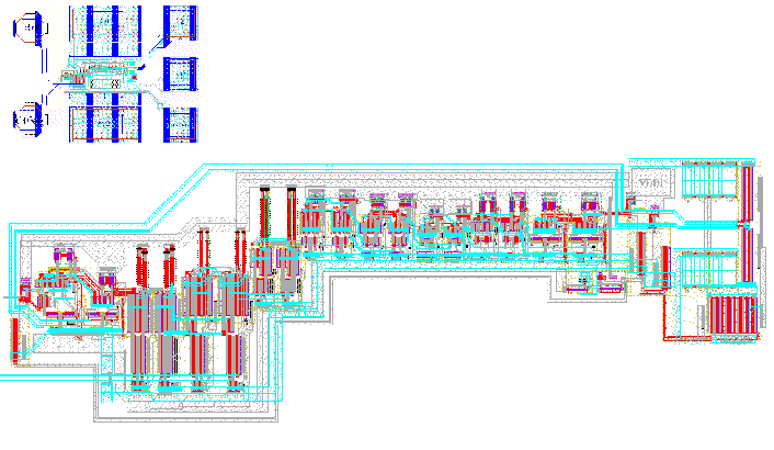
new prescaler layout
back to top
Designed Prescaler Circuits
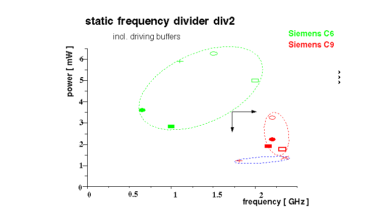
prescaler performance summary
| technology | frequency | power | comments |
|---|
| CMOS 0.25 m m | 9.5 G | 8 mW@2.5V | div128/129 cycle stealing method, power down |
| CMOS 0.25 m m | 7.5 G | 18 mW@2.5V | div128/129 standard, power down |
back to top
Opportunities for low power operation
bit synchron current switching
high speed FF power down
FF stacking / curren reuse at low speed
logic power down options ( hard redundance architecture )
output driver power control circuit
back to top
Next Steps
verify MOS models @ 1 ... 3 GHz by measurement
investigation of new architectures
optimize input driver
optimize init / control logic / div32
introduce current save techniques to the ring structure
layout generation / parasitic extract / parasitic simulation
implementation of standby mode
investigations to dynamic prescaler opportunities
back to top
[MIPI Homepage]
Kontakt: mailto: 